20,000+
Annual Capacity
Annual semiconductor sample-processing capacity.
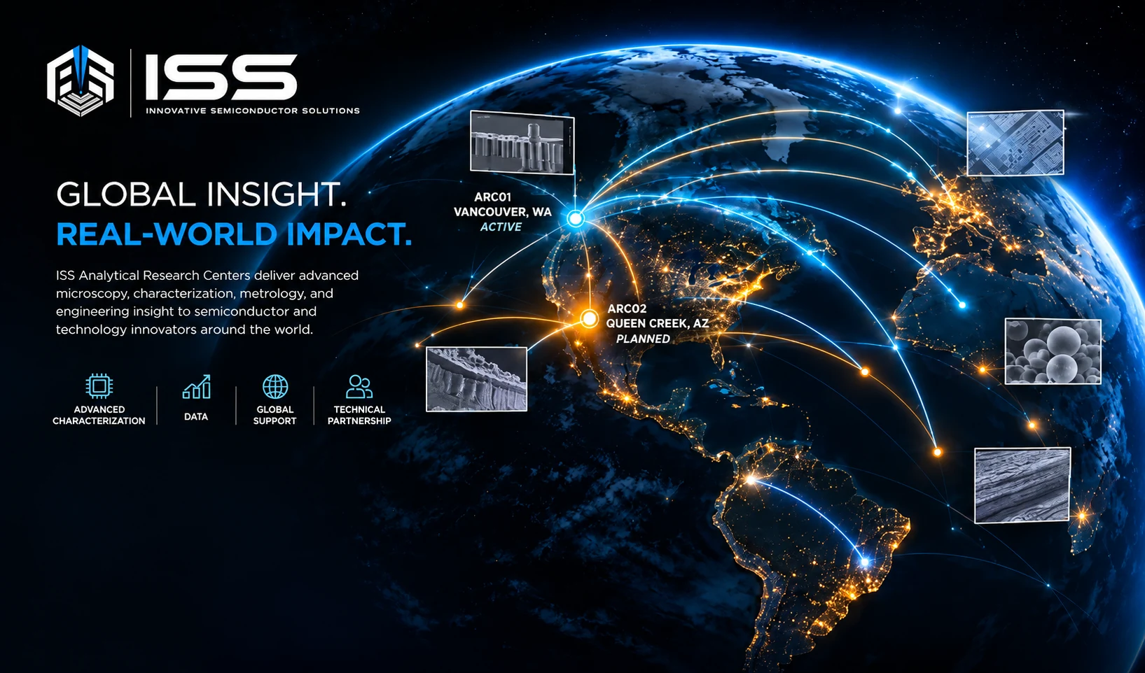
Global Insight. Real-World Impact.
ISS Analytical Research Centers help engineers understand the materials, devices and physical evidence behind safer transportation, reliable aviation, cleaner energy, advanced computing and the technologies shaping modern life.
Operational Performance
Our production workflow is designed to move samples quickly while maintaining the quality and repeatability complex analytical work requires.
Annual semiconductor sample-processing capacity.
Samples processed year to date.
Average sample turnaround time (TAT).
Current average rework rate.
How ISS Impacts the World
The work may begin with a cross section, a failure site, a material interface or an atomic-scale image. The value shows up in the products and systems people trust every day.
ISS provides analytical evidence and engineering support. Product safety, certification and final design decisions remain the responsibility of the product manufacturer and system owner.
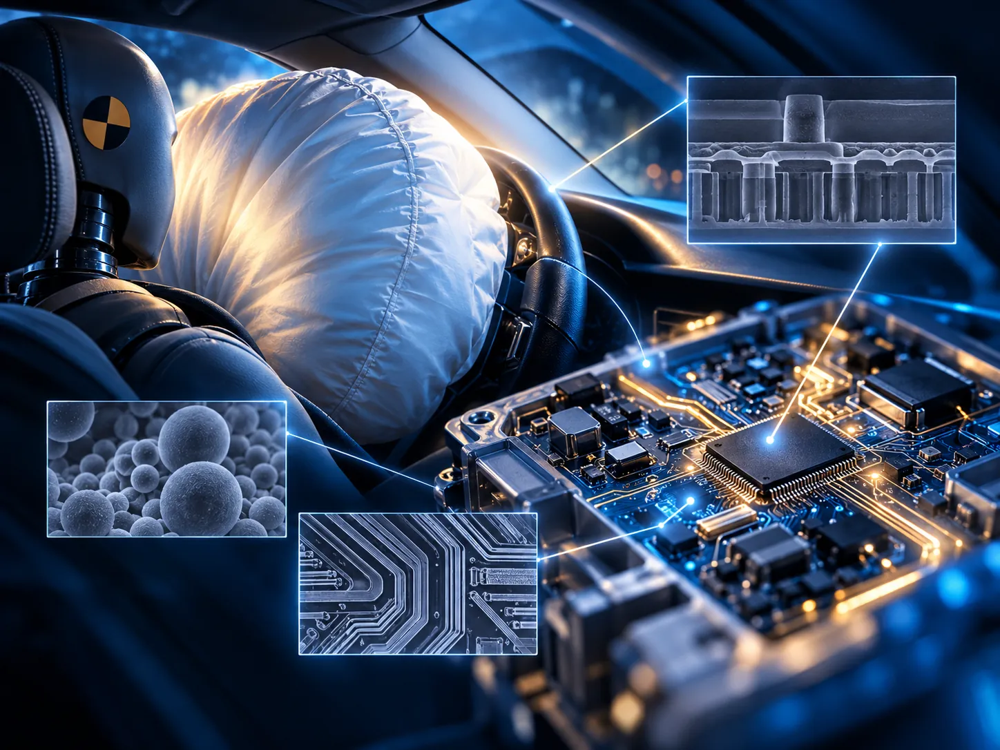
From airbag and sensing electronics to power devices and control systems, physical analysis can help identify defects, material changes and failure evidence.
Automotive & Power →
Microscopy, failure analysis and physical assurance can support avionics, communications, control electronics and other mission-critical hardware.
Aerospace & Defense →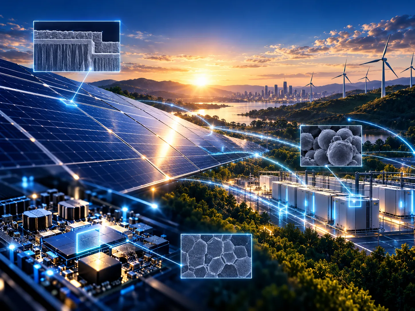
ISS analysis can support solar, power-conversion and energy technologies by revealing interfaces, degradation, materials behavior and device-level failure evidence.
Battery & Energy →Explore ISS
The homepage tells the impact story. The rest of the site provides the technical depth.
Advanced microscopy, failure analysis, metrology, circuit edit, sample preparation and physical assurance.
How We InvestigateTEM/STEM, SEM, FIB-SEM, EDS, EELS, diffraction, tomography and analytical measurement.
Where It MattersSemiconductor, AI, automotive, aerospace, energy, materials and emerging research markets.
What Needs SolvedVoiding, cracking, contamination, dimensional variation, failure localization and other physical-analysis problems.
Where We WorkA growing network of specialized ISS Analytical Research Centers with complementary expertise.
A Growing Analytical Network
ISS is building a distributed network of specialized Analytical Research Centers, each designed around complementary analytical capabilities and a common ISS operating model.
FIB-SEM · Metrology · Failure Analysis · TEM-STEM
ARC02 · PLANNEDCircuit Edit · Advanced Characterization · TEM-STEM · Security
FUTURE ARCSecond Materials Research Center supporting ARC01.
FUTURE ARCGeological & Earth Materials research specialization.
FUTURE ARCBiological & Life Sciences research specialization.
Start with the question.
Capabilities
Six integrated service lines support semiconductor engineering from physical access and high-resolution imaging through measurement, failure analysis, circuit modification and authorized hardware assurance.
Not sure where to start?
Technologies
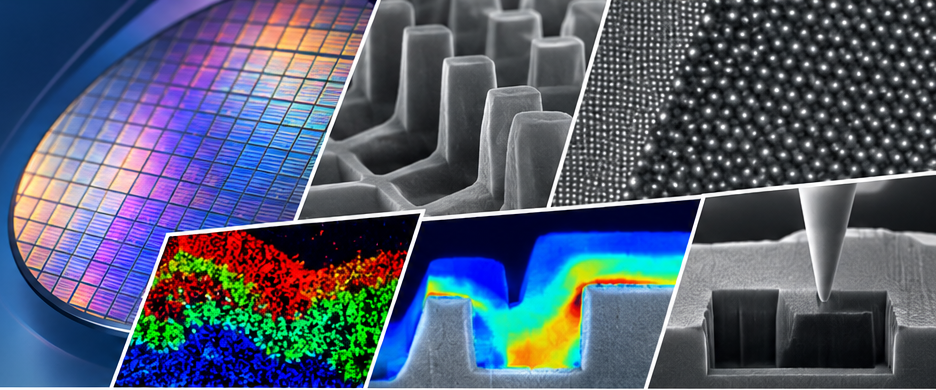
ISS combines imaging, preparation, spectroscopy, diffraction, metrology and analytical workflows to reveal structure, composition, dimensions and failure evidence across multiple scales.
Analytical Technologies
Rapid visual inspection and documentation for surface features, defects, contamination, and sample condition prior to advanced analysis.
High-resolution surface imaging for morphology, defects, structures, particles, and semiconductor device characterization across a wide range of sample types.
Precise dimensional measurement of critical features for process monitoring, device characterization, and semiconductor manufacturing support.
Site-specific cross-sectioning, material removal, circuit access, and advanced sample preparation using focused ion beam and dual-beam microscopy.
Atomic- and nanoscale imaging for detailed structural, defect, interface, and materials analysis using transmission and scanning transmission electron microscopy.
Elemental identification and compositional analysis through energy-dispersive X-ray spectroscopy, including point analysis, line scans, and elemental mapping.
Crystallographic analysis for phase identification, grain orientation, texture, grain boundaries, and microstructural characterization.
Advanced chemical and electronic structure analysis at the nanoscale using electron energy-loss spectroscopy in the TEM/STEM.
Three-dimensional reconstruction of internal structures, interfaces, defects, and material distributions using sequential imaging and computational reconstruction.
What do you need to know?
Technique Comparison
| Technique | Best For | Structural Info | Chemical Info | Dimensional Data |
|---|
One question may require more than one tool.
Industries
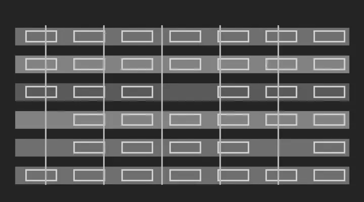
From semiconductor devices and AI infrastructure to energy systems, advanced materials and emerging research markets, ISS combines microscopy, characterization, metrology and engineering analysis to answer complex physical questions.
Markets We Serve
Connected Network
ISS is building each Analytical Research Center around a distinct technical role. Semiconductor and materials work is anchored by Vancouver; Queen Creek expands modification, characterization and security; future centers extend the network into materials research, geological research and biological sciences.
Start with the market and the question.
Common Analysis Challenges
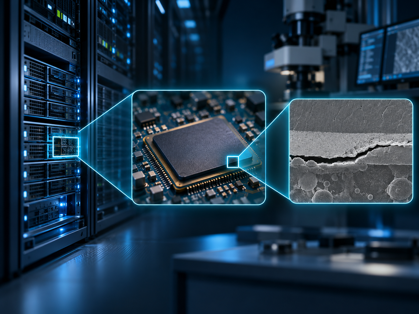
You do not need to know the instrument or analytical method before contacting ISS. Start with the physical question, failure signature or measurement challenge. ISS will build the analytical path around the evidence required.
Common Challenges
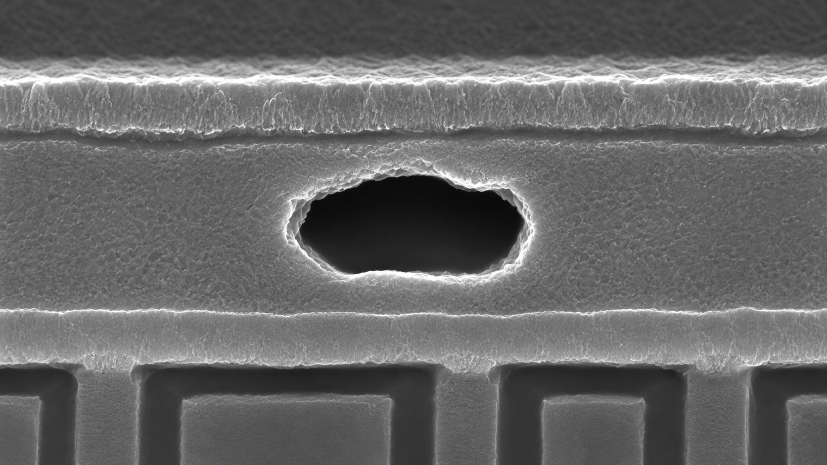
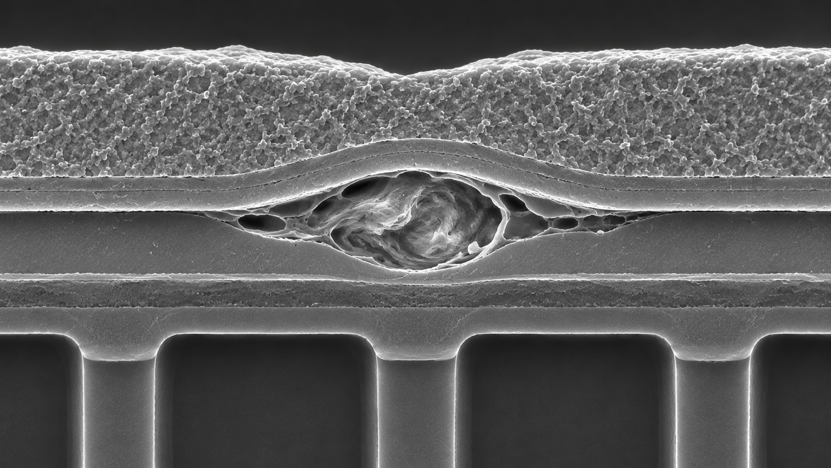
Locate and quantify voids in packages, interfaces, films, solder structures and advanced materials.
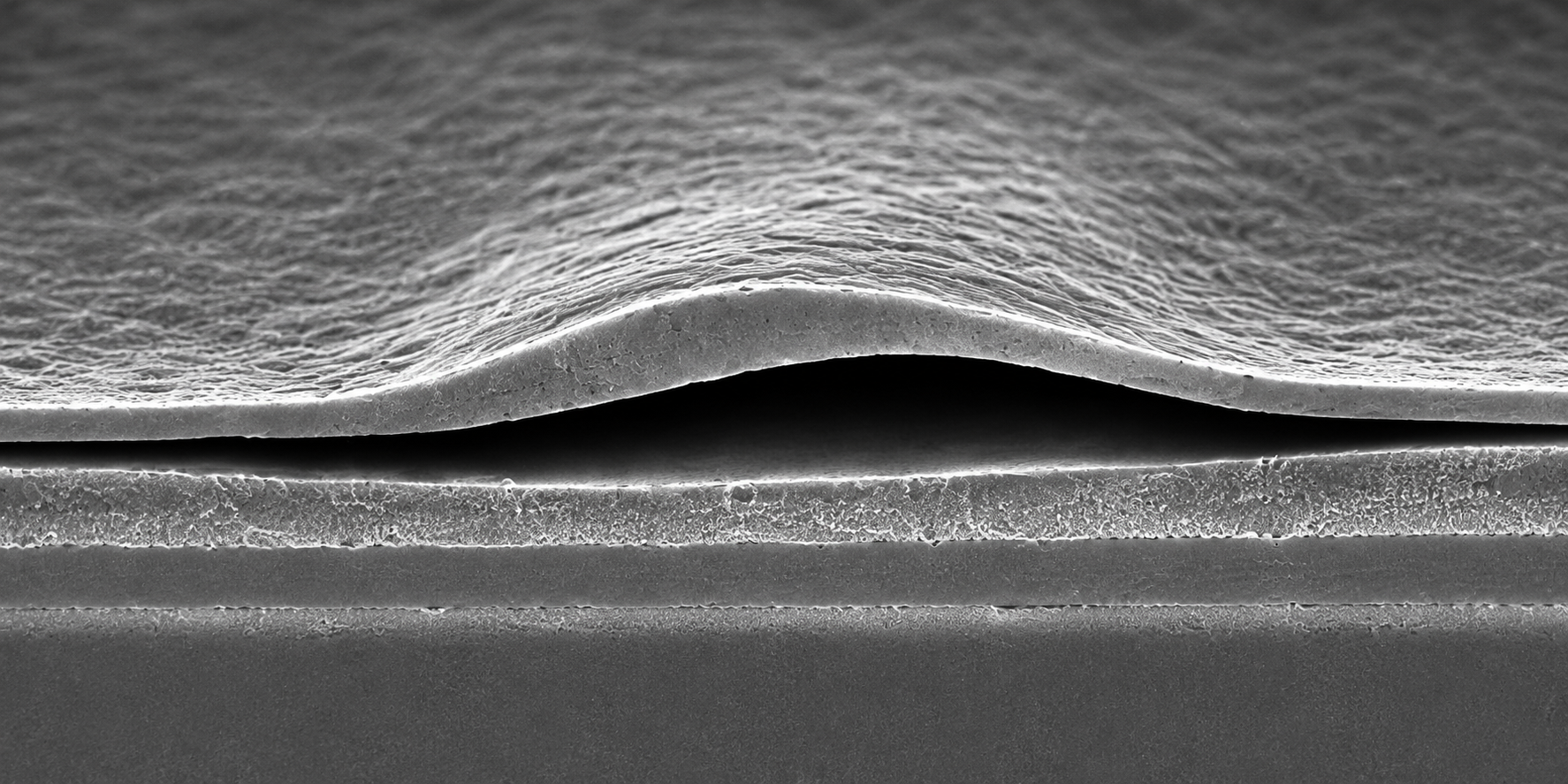
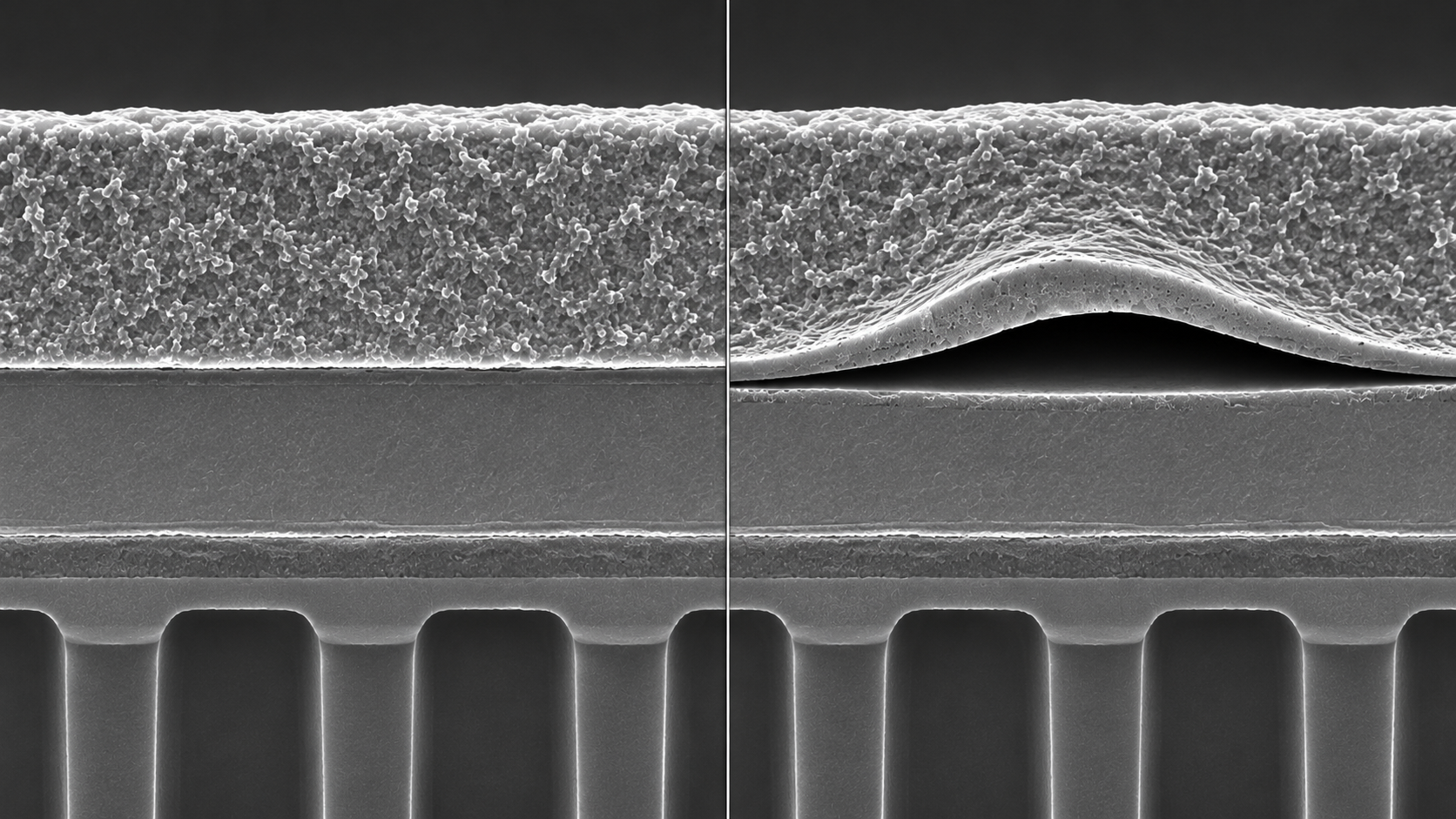
Evaluate separation, weak bonding, interface quality and failure propagation across layered structures.
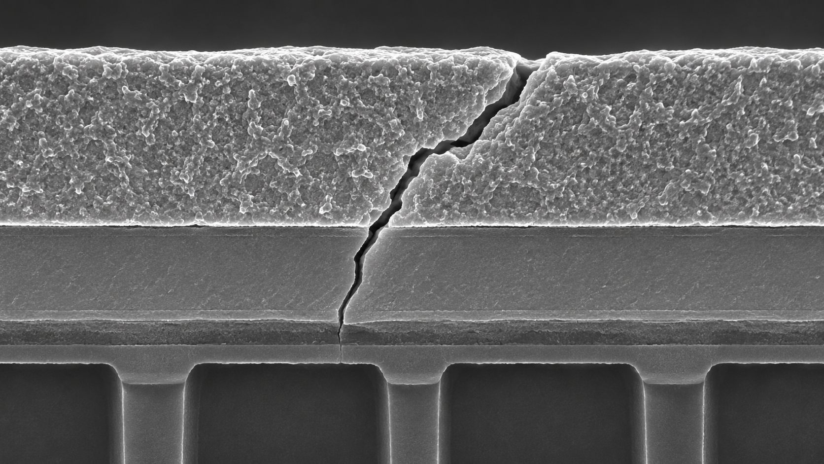
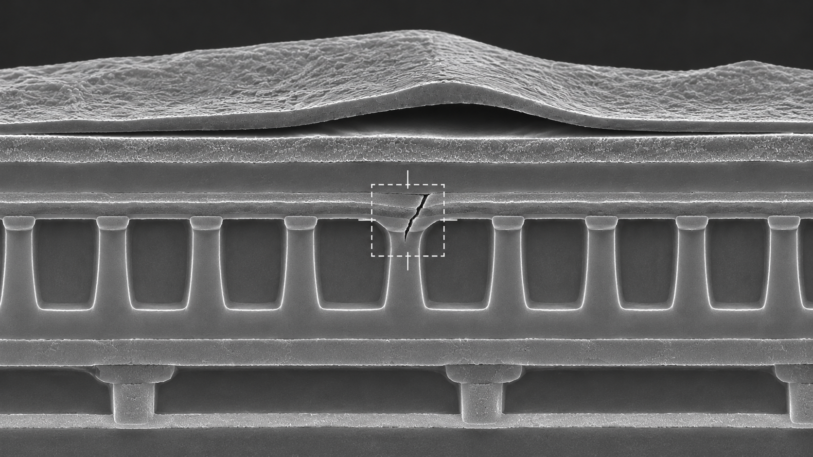
Identify crack initiation, propagation paths and surrounding structural evidence in devices, packages and materials.
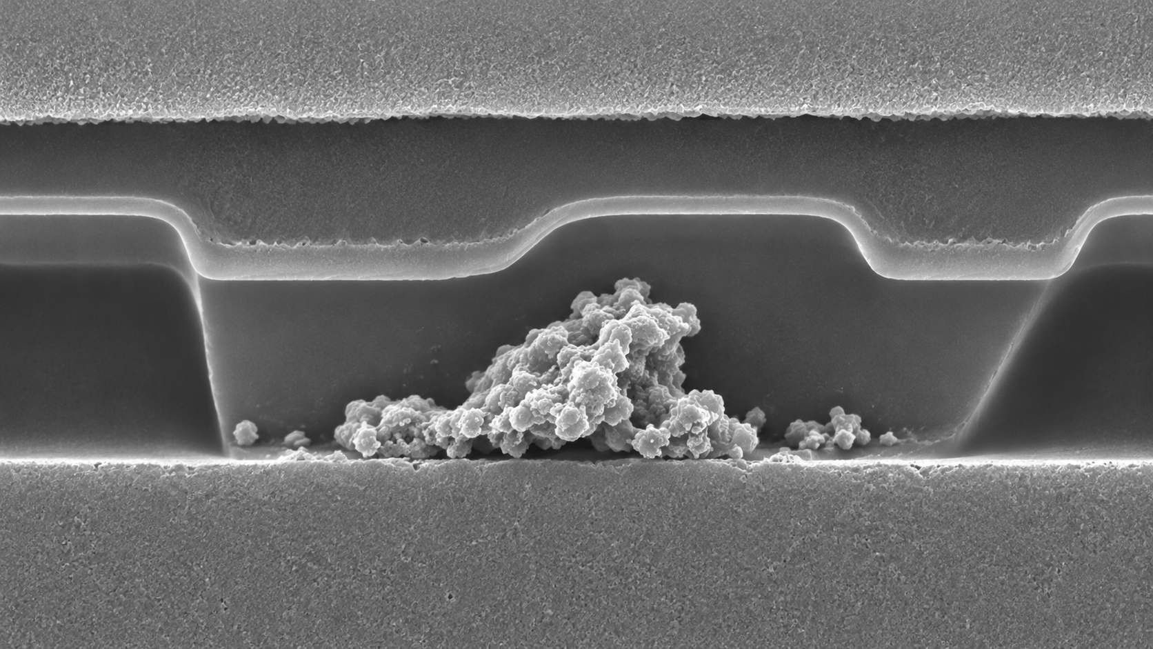
Locate particles or unexpected material and determine elemental composition with microscopy and spectroscopy.
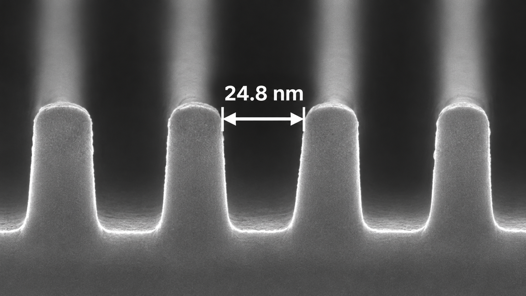
Measure linewidths, spacing, pitch, vias, trenches and other customer-defined geometric features.
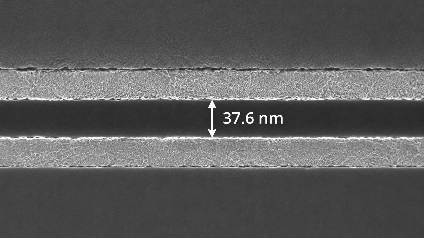
Quantify thin films, multilayer stacks, barriers, coatings and complex interfaces from SEM through TEM/STEM.
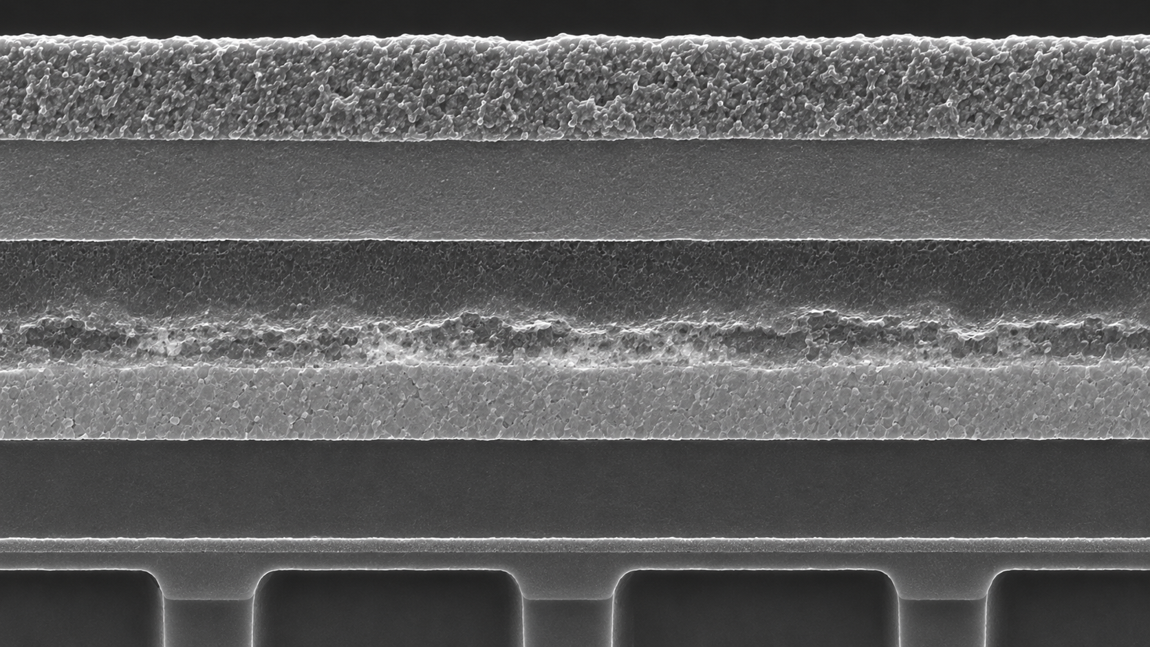
Characterize bonding, morphology, chemistry and structural transitions across critical interfaces.
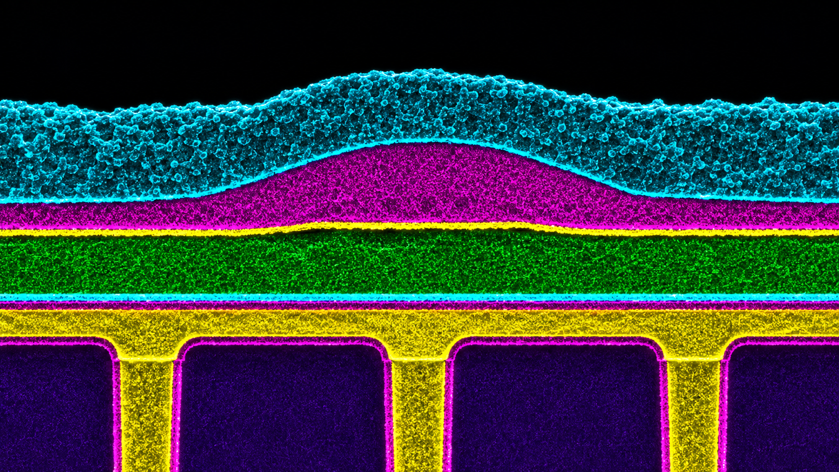
Use EDS and related analytical methods to identify composition and map elemental distributions.
Move from system-level symptom to the physical region requiring higher-resolution investigation.
Physically alter or access circuitry to test hypotheses, isolate paths and support engineering debug.
Compare failing or abnormal material against known-good devices, structures or process conditions.
When the failure mode is unclear, ISS can build a staged workflow to preserve evidence and escalate resolution as needed.
How ISS Approaches the Problem
Describe the symptom, device, sample condition and what decision the analysis needs to support.
Use optical, SEM, electrical context or prior evidence to narrow the investigation.
Move through FIB-SEM, TEM/STEM, EDS/EELS, metrology or circuit edit based on the evidence required.
Compare, measure and document the physical result in a form engineers can act on.
Related Paths
See what ISS provides, from failure analysis and metrology to circuit edit and sample preparation.
Explore TEM/STEM, SEM, FIB-SEM, EDS, EELS, diffraction, tomography and related methods.
See how ISS supports semiconductor, AI, automotive, aerospace, energy, materials and emerging research markets.
Not sure what technique you need?
ISS Analytical Research Centers
ISS Analytical Research Centers bring specialized microscopy, analysis, modification and physical-device assurance closer to the engineering teams that need them. Each ARC shares a common ISS operating model while developing a distinct technical specialization.
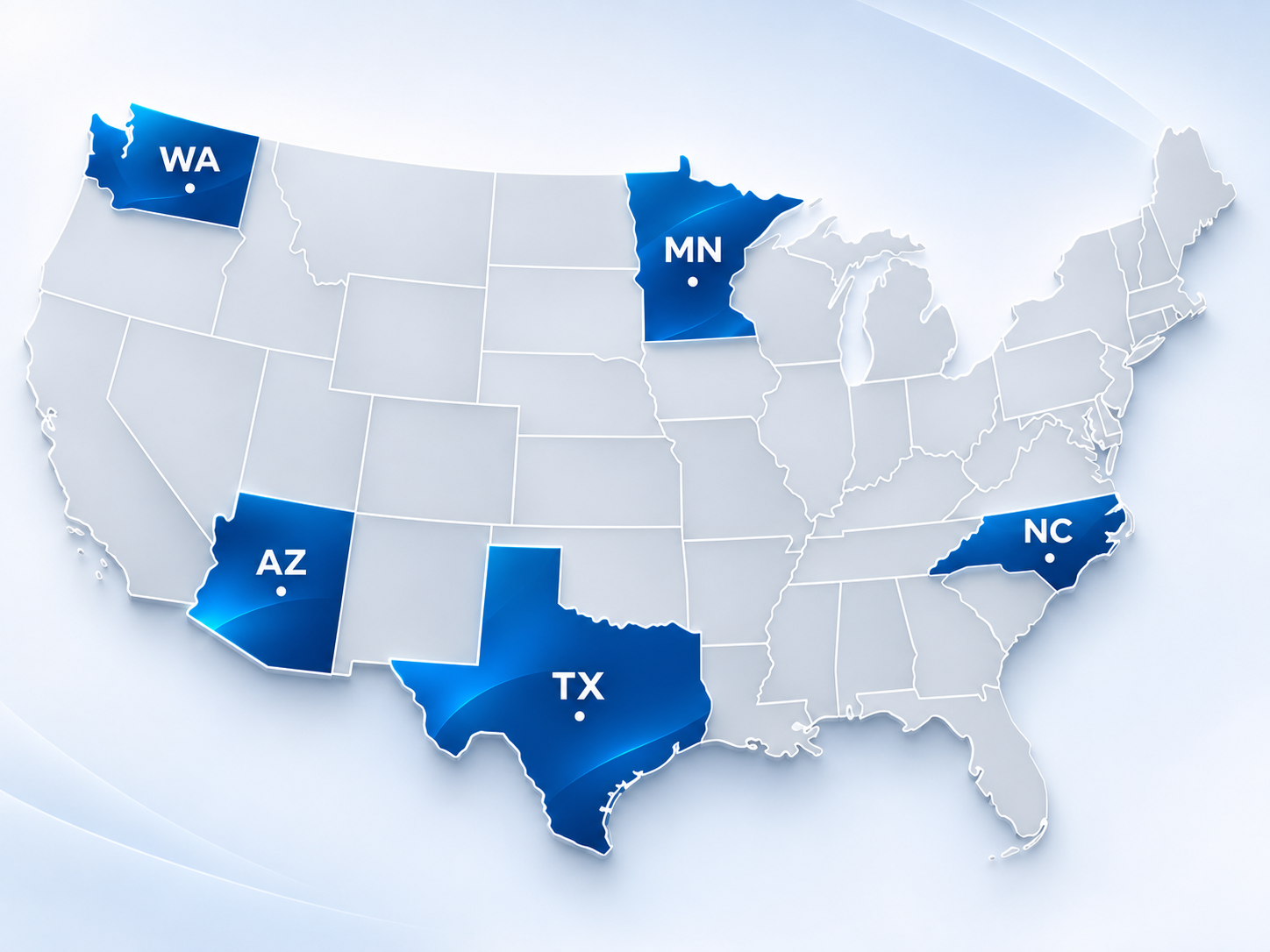
The ARC Network

Vancouver is the structural-analysis and failure-investigation hub of the ARC network, combining site-specific access, quantitative measurement and high-resolution microscopy.

Queen Creek is planned as the modification, advanced-characterization and physical-security hub of the ARC network, complementing Vancouver with specialized engineering capabilities.
Future Expansion
The following markets are future ARC expansion targets and are not currently presented as operating facilities.
Future ARC
Materials Research Center
A second materials-focused center intended to expand research capacity, provide network redundancy and support ARC01 Vancouver.
Future ARC
Geological & Earth Materials
Planned around geological materials, mineral and earth-material research, and advanced physical characterization.
Future ARC
Biological & Life Sciences
Planned as the network's biological and life-sciences research specialization as ISS expands beyond its semiconductor core.
One network. Multiple specialties.
ARC01 · Vancouver, Washington
The Vancouver ARC is ISS's flagship center for FIB-SEM, semiconductor metrology, failure analysis and TEM-STEM workflows.
Active ARC
Vancouver Specialization
Site-specific cross-sectioning, buried-feature access, serial investigation and preparation for downstream analysis.
Critical dimensions, layer thickness, pitch, geometry and recurring process-monitoring measurements.
Evidence-driven investigation connecting symptoms with structural, material and process observations.
High-resolution internal structure, interfaces, defects and analytical characterization at nanometer-to-atomic scales.
Integrated Vancouver Workflow
Vancouver is designed for investigations where physical localization, controlled preparation, quantitative measurement and high-resolution microscopy must work as one coordinated path.
ARC01 · Vancouver
ARC02 · Queen Creek, Arizona
The planned Queen Creek ARC is being positioned around circuit edit, advanced characterization, TEM-STEM and silicon security / physical assurance.
Planned ARCQueen Creek Specialization
Precision cut, isolate, deposition, access and engineering-debug workflows using dedicated circuit-edit technology.
Complementary analytical techniques including elemental, chemical and crystallographic characterization as projects require.
Nanoscale and atomic-scale imaging for device structures, interfaces, materials and security-sensitive investigations.
Authorized invasive hardware assessment, physical-device assurance, secure teardown and FIB-based security validation.
Integrated Queen Creek Workflow
Queen Creek is planned as a complementary ARC for projects that require active physical modification, deeper analytical characterization and authorized security evaluation.
ARC02 · Queen Creek
About ISS
Innovative Semiconductor Solutions is building a specialized network of Analytical Research Centers focused on helping engineers and researchers understand increasingly complex devices, materials, structures and failures across semiconductor and advanced research markets.
Built around the engineering question
Complex semiconductor problems rarely fit neatly into a single analytical technique. ISS brings complementary preparation, imaging, spectroscopy, metrology and engineering capabilities together so customers can move through an investigation without unnecessary handoffs.
Prepare → Image → Measure → Analyze → Understand

Our Approach
What happened, what changed, what must be measured and what decision must the data support?
Handle, prepare and document the sample in a way that protects the information it contains.
Choose the appropriate combination of preparation, microscopy, spectroscopy, metrology and analysis.
Provide organized data, observations and findings engineers can use.
Support both unique investigations and repeatable production-oriented analytical programs.
Use disciplined handling and confidentiality practices for customer devices and intellectual property.
A partner, not just a lab.
Careers at ISS
Build hands-on technical skills in a laboratory where precision, curiosity and teamwork turn complex devices into useful engineering answers.
Open Positions
We are hiring two Prep Technician Level 1 team members for our Vancouver Analytical Research Center. This is an entry-level technical role for people who take pride in careful hands-on work and want to grow in semiconductor analysis.
Build a Technical Career
Build strong fundamentals in handling, sectioning, polishing and analytical readiness.
Develop toward increasingly complex, site-specific and microscopy-driven preparation methods.
Expand technical understanding around imaging, measurement and analytical workflows.
Grow with a company building specialized Analytical Research Centers across multiple markets.
Equal Opportunity
ISS considers qualified applicants without regard to race, color, religion, sex, national origin, age, disability, veteran status, or other status protected by applicable law.
Ready to build something technical?
Resources
Explore capability documents, technical guides, application notes and sample-submission resources.
Overview of advanced microscopy, failure analysis, sample preparation and analytical capabilities.
Request / Download →Overview of physical-security evaluation and semiconductor assurance services.
Request / Download →How to identify, document and prepare samples for ISS technical review.
View Guide →Understand what each technique reveals and when each is appropriate.
Explore →How targeted preparation connects a customer-defined feature to advanced microscopy.
Explore →How microscopy can support semiconductor CD and cross-sectional metrology.
Explore →Need help selecting a technique?
Private Equipment Marketplace
ISS maintains a private marketplace for qualified buyers evaluating pre-owned SEM, FIB-SEM, TEM and STEM systems. Current inventory, pricing, system configuration details and availability are shared only after access is approved.
Request Access
To protect active opportunities and confidential equipment transactions, ISS no longer publishes its equipment catalog or pricing publicly. Approved buyers receive direct access to current listings and can work with ISS on configuration, logistics, installation, service and warranty options.
Send your company name, equipment interest and intended application to ISS Equipment Sales.
ISS confirms the request and determines which current systems are relevant to your application and facility requirements.
Qualified buyers receive current availability, pricing, configuration details and direct support from ISS.
ISS can review detector packages, analytical options, facility requirements and intended applications before purchase.
Turnkey packages can include deinstallation, shipping coordination, installation, startup and acceptance support as quoted.
Warranty and service terms are defined for each system. Covered FRU parts and excluded consumables are identified in the equipment agreement.
Secure Client Access
ISS uses client-approved SharePoint environments for secure storage and transfer of sensitive project data. Client workspaces remain protected by the access controls established for each engagement.
Secure Data Workflow
Project files, reports, images and sensitive data can remain within the SharePoint environment approved for the engagement.
Access is limited to authorized users and governed by the permissions established for the client workspace.
The public site provides navigation and project intake; sensitive project data does not need to be stored on the public website.
Need access?
Secure Employee Access
ISS employee resources are accessed through the company-approved Microsoft 365 and SharePoint environment. Use your ISS-issued credentials to access authorized internal resources.
Internal Access
Internal documents, procedures and authorized employee resources remain within the company-approved Microsoft environment.
Employees should use only their ISS-issued account and the access permissions assigned to their role.
This login page is the starting point for a future employee portal that can organize SOPs, training, schedules, equipment status and internal resources without moving sensitive information onto the public website.
ISS Team Access
Submit a Project
You do not need to know which microscope, preparation method or analytical technique your project requires. Start with the sample and engineering question.